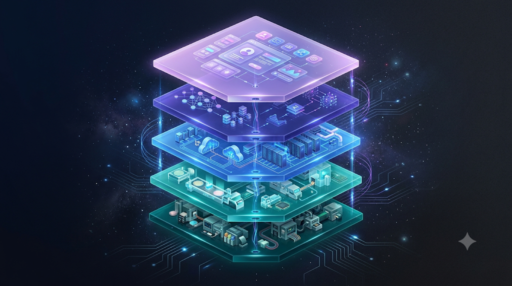
AI Industry Structure, Layer 2: Foundries
No matter how brilliant a GPU NVIDIA designs, it’s just a blueprint without a factory to actually stamp it out. Foundries, the final piece of Layer 2 in the AI industry structure, are exactly where that blueprint becomes a physical product. In this article, we’ll cover exactly what a foundry does. We’ll also look at why Taiwan’s TSMC effectively holds a monopoly on this market, and why Samsung and Intel can’t catch up.
Revisiting Foundries
Foundries are the most capital-intensive layer in the semiconductor industry. Building a single state-of-the-art plant (fab) costs tens of billions of dollars, and even completing it takes years. That’s why the number of companies in the world that can newly enter this market can be counted on one hand.
Why Design and Manufacturing Split
Chip design (fabless), which we covered earlier, is split apart from foundries (production). That split reveals something important about this industry: design and manufacturing are run as two completely separate businesses. There’s a company that’s great at design (NVIDIA) and a separate one that’s great at production (TSMC). Each is only half the story without the other.
Why Can’t Anyone Catch TSMC?
Making a cutting-edge chip comes down to a technology called process technology. It refers to how thin a circuit line can be drawn. The smaller the number (say, 3nm or 2nm), the more transistors fit into the same area, which improves performance and power efficiency. At this leading edge, TSMC is widely seen as having a noticeably higher yield than Samsung or Intel. Yield refers to the ratio of chips made without defects.
What makes the yield gap so consequential is that a low yield makes the cost of a single chip shoot up. Big customers like NVIDIA have no choice but to pick whoever can deliver stable, large-scale production. That structure keeps pulling business toward TSMC. This industry has a “snowball effect,” where a technology gap that opens up once just keeps widening.
The Numbers Make the Gap Even Clearer
As of Q1 2026, TSMC’s foundry market share stood at 72.3%, up from the previous quarter’s 70.4%. Samsung Electronics, in second place, managed only 6.5% — a gap of more than 10x. Intel’s foundry business is still so early-stage that it doesn’t even show up on this leaderboard yet.
This gap gets even clearer when you look at yield on the latest 2nm process. TSMC is reportedly above 80%, while Samsung is said to sit in the 50-60% range. Industry estimates even put TSMC’s share of the AI accelerator (GPU, etc.) market at roughly 95%. Big customers like NVIDIA, AMD, and Broadcom have all flocked to TSMC as a result.
Foundries Are Also a Geopolitical Issue
Most of the world’s leading-edge chips are made on a single island, Taiwan. That fact gets treated as a national security issue, not just an industry one. It means that if geopolitical tension flares up around Taiwan, the entire global AI industry could be shaken. This is often called the “Silicon Shield.” The idea is that Taiwan holding the keys to chip production functions as a kind of security insurance in itself.
That’s why the U.S. government has been strongly pushing TSMC and Samsung to build factories on American soil. The goal is to reduce this risk. That said, U.S. plants are widely seen as still lagging behind Taiwan’s mainland facilities in yield and cost competitiveness. For now, a two-track structure — “leading-edge production in Taiwan, some volume in the U.S.” — will likely continue.
What Investors Should Watch For
The technical bar in foundries is so high that it’s important to keep tracking these three things.
Once a technology gap opens up in foundries, it rarely closes within just a few years. That means “today’s leader staying the leader” is more likely here than in most other layers.
Closing Thoughts
Foundries aren’t very visible in the AI industry structure, but they may actually be the most irreplaceable layer of all. No matter how good a design is, it means nothing without a factory to physically produce it. Only a handful of factories in the world can do that.
So how does this factory actually etch such microscopic circuits? In the next article, we’ll wrap up the Layer 2 series and move on to Layer 1: materials and equipment. We’ll cover why ASML’s EUV photolithography machines are called the industry’s “chokepoint.”
We cover why ASML’s EUV photolithography machines are called the industry’s “chokepoint.”