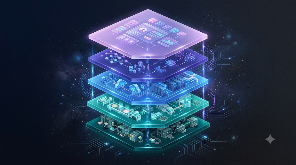
AI Industry Structure, Layer 1: Materials & Equipment
No matter how great a foundry TSMC is, it can’t make anything without the equipment to actually etch circuits. Materials and equipment, the very bottom layer of the AI industry structure, is where those tools and raw materials come from. In this article, we’ll cover why a single Dutch company, ASML, is called the industry’s “chokepoint.” We’ll also look at what materials, beyond equipment, are needed. This article wraps up the “5 Layers of the AI Industry” series, from Applications all the way down to Materials & Equipment.
Revisiting Materials & Equipment
We’ve now worked our way all the way down the AI industry structure, from Layer 5 to Layer 1. We covered applications, AI models, infrastructure and cloud, and chip manufacturing. At the very bottom of all of it sits this equipment and these materials. No matter how great a foundry like TSMC is, it can’t even get started without the right equipment. It also needs the raw materials to etch a circuit.
Why Is ASML Irreplaceable?
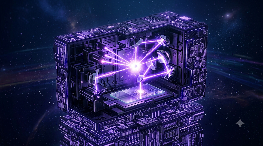
The latest chips require EUV (extreme ultraviolet) photolithography machines. Exactly one company in the world makes them: the Netherlands’ ASML. Without this equipment, neither TSMC nor Samsung can make the latest chips. That’s why this layer is called the industry’s “chokepoint.”
Here’s what an EUV machine actually does. It fires a laser at a tiny droplet of tin 50,000 times a second, instantly generating plasma. It then bounces the extreme ultraviolet light that plasma gives off across ultra-precise mirrors multiple times. That etches a circuit pattern onto the wafer. Reliably generating plasma hotter than the sun, 50,000 times a second, is a feat only ASML has managed to pull off.
Interestingly, even ASML doesn’t build this machine entirely on its own. 85% of an EUV machine’s components come from outside partners. Germany’s Zeiss makes the ultra-precise mirrors that reflect the light. Cymer, a company ASML fully acquired, makes the laser light source. ASML’s real strength isn’t the technology to build components itself. It’s the ability to integrate thousands of partners scattered across the globe into a single machine. A supply chain built up over more than 30 years like this can’t be copied overnight just by having money. Industry observers note that even as China tries to domesticize semiconductor equipment production, it likely remains 10-15 years behind.
Beyond Equipment, There Are Materials Too
If equipment is the “machine,” materials are the “ingredients” that machine consumes every day. There are three main types.
The wafer (a silicon disc) is the thin, round plate that a chip is built on. It’s made by extracting silicon from sand (silicon dioxide) and refining it to ultra-high purity. That refined silicon then gets grown into a cylinder and sliced thin. Photoresist is a chemical that reacts to EUV light. It lets the wafer’s surface be etched away in the shape of the circuit. Various specialty gases are also used throughout the process, to clean or etch the wafer.
These materials don’t get as much buzz as the equipment. But if the supply of even one of them is cut off, an entire foundry grinds to a halt. Production of semiconductor-grade specialty gases and materials is often concentrated in a specific country or company. As a result, this layer often gets brought up as a kind of “weapon” whenever trade tensions flare up between countries.
What Investors Should Watch For
This layer comes closest to being the most irreplaceable “single point of failure” in the entire AI industry structure. That’s exactly why investors should watch the following.
Companies in this layer might not look directly connected to the AI boom. But as AI chip production itself increases, this is actually the layer that benefits first, and most reliably. Foundries have to buy more of this equipment before they can even expand their factories.
Closing Thoughts
Materials and equipment is the least visible layer in the AI industry structure, but it’s actually where everything starts. Raw material that’s essentially sand passes through this equipment and becomes a wafer. It passes through a foundry and becomes a chip. It meets a fabless company’s design and becomes a GPU. It combines with memory, CPU, and storage and becomes a server. It passes through cloud, cooling, power, and networking and becomes a data center. An AI model gets trained on top of that. And finally, it reaches you through the screen of an application.
With that, the “5 Layers of the AI Industry” series comes to a close. Applications → AI Models → Infrastructure & Cloud (cloud, cooling, power, networking) → Chip Manufacturing (memory, CPU, storage, GPU and chip design, foundries) → Materials & Equipment. We hope this chain, covered across 10 articles, has helped you understand AI-related stocks. If you’d like to revisit the full picture, head back to The 5 Layers of the AI Industry: Overview.