AI Industry Structure, Layer 3: Networking & Optics
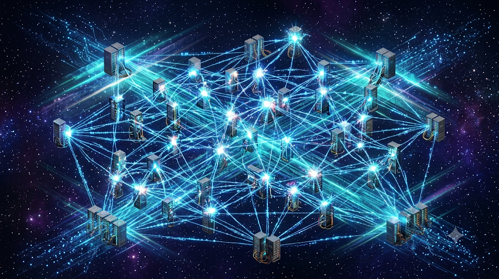
No matter how good a single server is, it can’t train a large AI model on its own. So data centers wire together tens of thousands of GPU servers with dense networking and optics infrastructure, making them behave like one giant supercomputer. Let’s start by covering why this networking and optics layer, the final piece of Layer 3 (Infrastructure & Cloud), has recently drawn attention on par with HBM.
Revisiting Networking & Optics
If this connection is too slow, even a huge pile of great GPUs ends up performing at only half capacity. When training a single AI model, tens of thousands of GPUs have to exchange their computation results with each other in real time, and this “exchange speed” directly determines how fast the entire training process runs.
InfiniBand vs. Ethernet: The Real Showdown
There’s one real technology showdown playing out right now in this layer, and it’s the hottest in the industry — the fight between InfiniBand and Ethernet. Both are communication standards for connecting servers, and InfiniBand has long reigned as the standard for AI clusters.
Lately, momentum has been shifting toward Ethernet. In 2025, an industry group called UEC (Ultra Ethernet Consortium) overhauled the standard and rapidly closed Ethernet’s performance gap, and companies like Meta have already reported training runs at the scale of 24,000 GPUs using Ethernet alone, reaching performance on par with InfiniBand. Even NVIDIA is hedging its bets, offering an Ethernet-based product (Spectrum-X) alongside its own InfiniBand switches.
Optics Are Moving Closer to the Chip
Lately, that distance has been shrinking. A technology called CPO (Co-Packaged Optics) pulls optical components right into the GPU package itself, working on a principle similar to how HBM sits right next to the chip. The goal is to cut down the conversion steps between optical and electrical signals, pushing data transfer speeds higher while also reducing power consumption.
NVIDIA and TSMC are leading this technology, and Marvell is out in front on the key chip (the DSP) that processes optical signals. In other words, optics itself is gradually evolving from “long-distance wiring” into a “chip-adjacent component.”
What Investors Should Watch For
This is a layer that could end up following a pattern similar to HBM. As AI server demand grows, components like optical transceivers could face shortages right along with it.
The thing to check is how far ahead this company is in supplying the latest generation of optical communication standards (transfer speed). The bandwidth AI data centers demand keeps growing, so whichever company mass-produces the next-generation standard first stays ahead.
Closing Thoughts
Cloud, cooling, power, and networking — we’ve now covered all four pieces of Layer 3 (Infrastructure & Cloud). It’s clear that even completing a single server takes this many moving parts working together.
Starting with the next article, we’ll move on to Layer 2: Chip Manufacturing. We’ll work through the hardware manufacturing supply chain that forms the foundation of the AI industry structure, one piece at a time — memory, CPUs, and storage, GPU design, and foundries.
We cover the whole memory hierarchy from registers to storage, and why HBM is such a hot topic.